Design of a PCB Hole
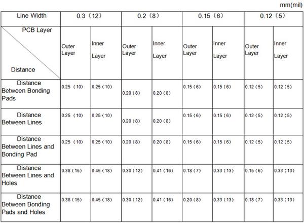
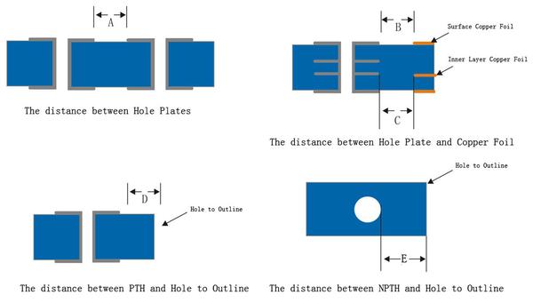
1. Design of Through Hole
Jun 05, 2015
Trace Impedance
Care should be taken to distinguish between single ended and differential trace impedance. High speed single ended signa...
Apr 21, 2015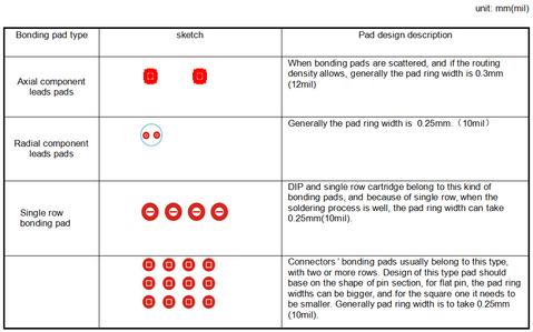
Bonding Pad Design Ⅰ
1.Design of bonding pad with through hole cartridge components a) The diameter design of components plug-in holes is acc...
Apr 10, 2015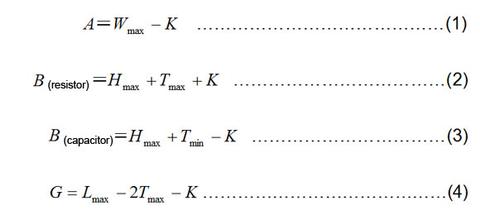
Bonding Pad Design Ⅱ
SMD component bonding pad design 2.1 Passive device pad design 2.1.1 Rectangle component pad design Shapes of resistor a...
Apr 09, 2015
Screen Printing Design
General requirements for screen printing 1. The line weight of screen printing should be greater than 6 mil, and make su...
Apr 09, 2015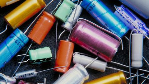
6 Suggestions for Engineers of Components Selection
There was a common phenomenon existing in products technical condition in some corporations: all developers condemned th...
Apr 09, 2015