Bonding Pad Design Ⅱ
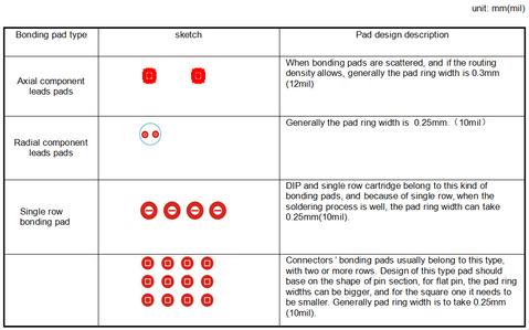
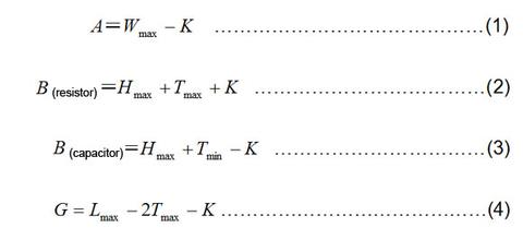
SMD component bonding pad design 2.1 Passive device pad design 2.1.1 Rectangle component pad design Shapes of resistor a...
Apr 09, 2015
Screen Printing Design
General requirements for screen printing 1. The line weight of screen printing should be greater than 6 mil, and make su...
Apr 09, 2015
6 Suggestions for Engineers of Components Selection
There was a common phenomenon existing in products technical condition in some corporations: all developers condemned th...
Apr 09, 2015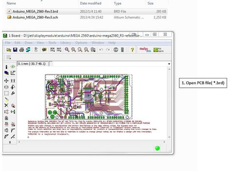
Export Drill File from Eagle2
After the design of a printed circuit board (PCB) completing, it needs to be sent to a PCB manufacturer to be fabricated...
Apr 09, 2015
What is a printed circuit board -- Basic PCB Concepts?
This article is from Electrosoft Engineering , it is useful to clarify the mind for new hand.
Mar 19, 2015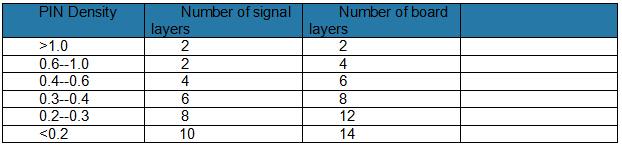
PCB Stack-Up Design
Before designing multi-layer PCB circuit boards, designers need to confirm the circuit boards structure primarily based ...
Mar 16, 2015